
Cerebras Couldn't Exist Without TSMC
A constraint-layer reading of the $95B IPO — and why the foundry partnership matters more than the wafer


The Cerebras team rings the Nasdaq bell on IPO day. Image: Cerebras Systems / Nasdaq
Cerebras rang the bell at NASDAQ on Thursday. CBRS opened at $350 — nearly double its $185 IPO price — and closed up 68% at $311.07, valuing the company at roughly $95 billion. Thirty million shares, $5.55 billion raised. The largest U.S. tech IPO since Uber in 2019. The largest pure-play AI IPO ever to hit public markets.
The LinkedIn feed lit up immediately. Foundation Capital, Eclipse Ventures, and Benchmark — who wrote the first term sheets in 2016 — held decade-long conviction in a non-consensus bet, and each earned their moment.
Steve Vassallo at Foundation Capital, who led the 2016 term sheet and has been on the board ever since, wrote the canonical insider account this week — a nineteen-year relationship with Andrew Feldman that finally got to ring the bell. Lior Susan at Eclipse captured the team frame as well as anyone: “Not another semiconductor company, but a team willing to defy a 75-year assumption about how computing should scale.”
Those framings are true. They’re earned. But they’re not the most important thing about this IPO.
Here’s what every celebration post is missing — and what matters most for the next decade of constraint-layer investing.
What everyone got right
Cerebras built something the industry had spent 75 years saying was impossible: a working, yieldable, commercially deployed wafer-scale processor.
The reason the industry said it was impossible was actually quite simple. When chips are manufactured, defects happen — a speck of dust, a microscopic flaw in the silicon crystal, random and statistically unavoidable. The bigger the chip, the higher the odds that at least one defect lands inside it and kills the entire thing. So for 75 years, every chip maker on Earth made the same bet: keep chips small. Stamp a single 12-inch silicon wafer with hundreds of small chip dies, cut them apart, discard the ones with defects, and ship the rest. NVIDIA’s flagship B200 compute die is roughly 740 mm² — about the size of a postage stamp.
Cerebras bet the entire company that this 75-year assumption was wrong. The Wafer-Scale Engine 3 is the size of a dinner plate, not a postage stamp — sixty-two times the area of NVIDIA’s current B200 flagship, packing 4 trillion transistors and 900,000 AI-optimized cores onto a single uncut wafer.
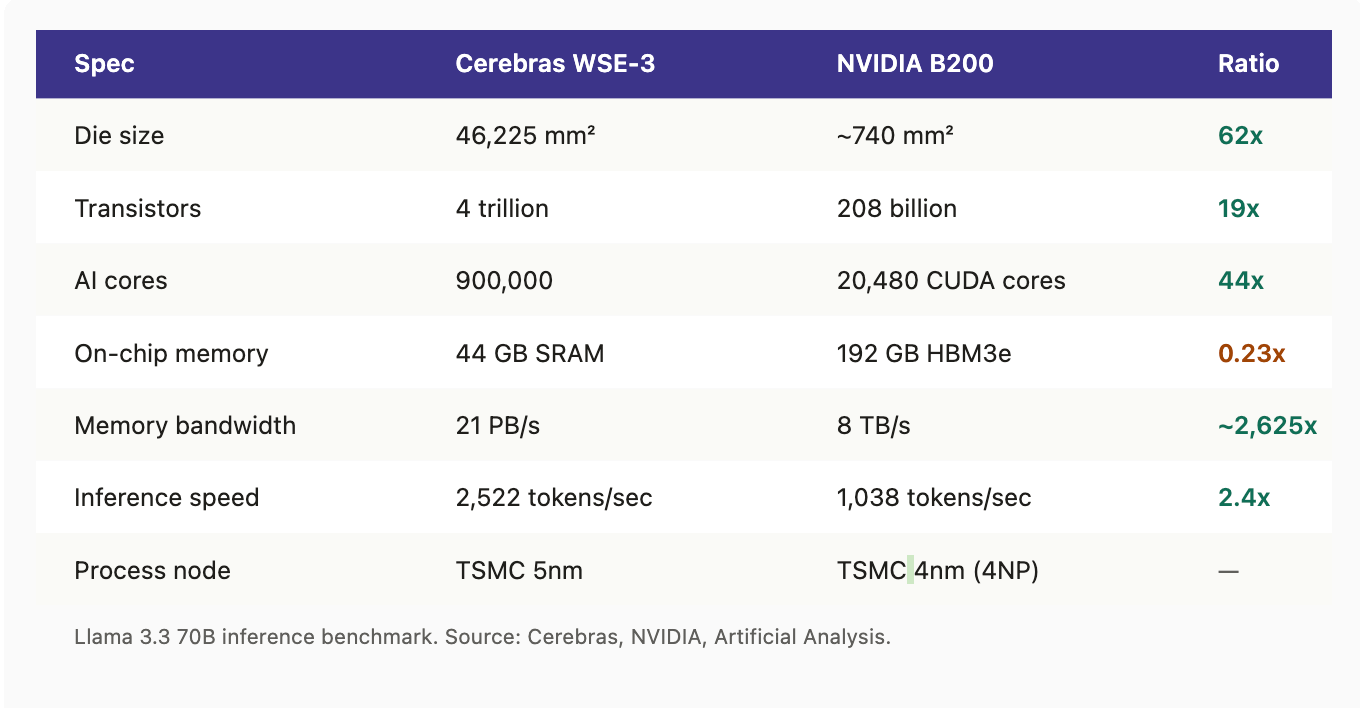
Spec-by-spec: Cerebras WSE-3 vs NVIDIA B200
The engineering courage required to attempt this is genuine. The fact that they actually shipped it is extraordinary. Andrew Feldman, Sean Lie, Gary Lauterbach, Michael James, and Jean-Philippe Fricker deserve every word of celebration they’re receiving this week.
But to understand why this IPO matters beyond a great team and a contrarian bet, you have to look at the constraint Cerebras was actually attacking.
The constraint Cerebras solved
Modern large language model inference is not compute-bound. It’s memory-bound.
As Steve Vassallo framed it in his decade-with-Cerebras post:
memory bandwidth, not raw compute, was the true constraint on what neural networks could achieve.
Generating each token requires moving all model weights from memory to the compute units. On a standard NVIDIA GPU, those weights sit in High-Bandwidth Memory chips connected to the processor by an interface that — fast as it is — caps the achievable token generation rate. The compute units sit idle waiting for memory. The bottleneck is bandwidth, not arithmetic.
Cerebras’s answer is brutally direct: hold every weight in on-die SRAM, physically distributed next to the cores. No off-chip memory trip. No inter-GPU networking penalty. The WSE-3 carries 44 GB of SRAM on the wafer itself, delivering memory bandwidth of 21 petabytes per second — roughly 2,625 times more than NVIDIA’s current B200 flagship.
That single ratio is the company’s entire thesis. Independent benchmarks bear it out: Llama 3.1 70B at over 2,500 tokens per second on Cerebras, versus a few hundred on the best GPU alternatives. For inference workloads — and especially for agentic AI workflows that require multiple low-latency model calls in sequence — that gap is the difference between a viable product and impossible economics.
What makes the bet most striking isn’t the engineering — it’s the timing. Cerebras committed to wafer-scale architecture in 2016, a decade before agentic AI, voice models, real-time coding agents, and reasoning models became the defining workloads of frontier AI. They built a chip purpose-engineered for low-latency, single-user inference at a time when “AI inference” mostly meant batch image classification. They saw a workload coming that didn’t yet exist as a major market, and they spent ten years preparing for it. By the time the market caught up — when agentic AI made tokens-per-second-per-user the binding economic metric — Cerebras was the only company in the world with hardware purpose-built for that constraint.
This is constraint-layer investing in its purest form: identify the binding bottleneck in a critical system, then back the founders willing to make a structurally heretical bet to eliminate it — sometimes years before the market knows the bottleneck exists.
Cerebras vs Groq — same constraint, two architectures
Cerebras isn’t the only company that saw this constraint. Groq’s LPU architecture solves the same memory-bandwidth problem with a different structural answer: many small chips with on-chip SRAM, networked together via deterministic interconnect. Cerebras’s answer is one big chip. Groq’s answer is many small chips behaving like one big chip.
I wrote about the NVIDIA-Groq acquisition when it closed, framing it as the first major M&A signal that the inference layer was being recognized as a distinct strategic asset. Both Cerebras and Groq are right. Both architectures genuinely bypass the memory wall that constrains GPU inference. Both have anchor customers underwriting their scale.
This is important for how to read the constraint layer as an investor: constraint-layer markets don’t converge on a single architecture. The bottleneck is real, and the demand is structural, which means the market is large enough to support multiple architecturally distinct winners. Cerebras dominates single-user inference latency on frontier models. Groq wins on developer adoption and deployment flexibility. SambaNova’s three-tier memory hierarchy serves the largest frontier models on the smallest hardware footprint.
The lesson isn’t “who beats NVIDIA.” It’s that the constraint is binding, the market is large, and multiple structurally-aligned bets will scale.
The TSMC observation almost nobody is making
Here’s the part missing from every congratulations post — and the part that matters most for understanding why Cerebras is investable at $95 billion, and why the next decade of constraint-layer investing will look different from the last.
Wafer-scale isn’t a new idea. Gene Amdahl tried it at Trilogy Systems in the 1980s. Multiple research labs and a handful of well-funded startups tried it in the 1990s and 2000s. Every one of them failed. The idea was never the bottleneck.
What Cerebras actually built — and what almost nobody is talking about this week — is a decade-long, deeply co-developed manufacturing process with TSMC that solved five separate problems each previously considered fundamental.
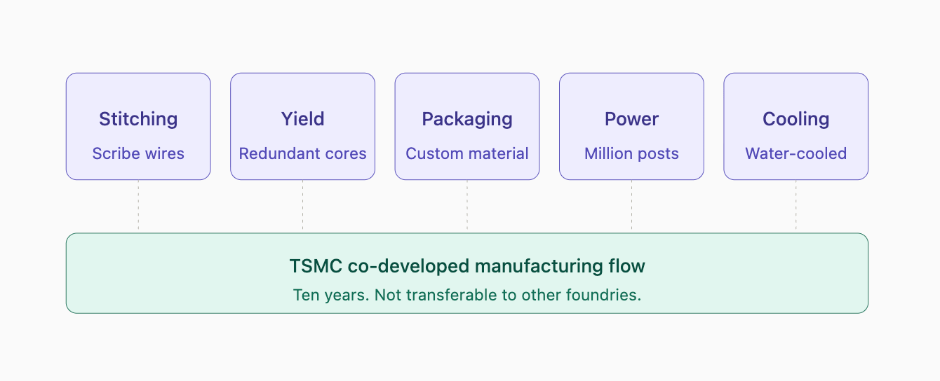
Five challenges, one platform: the TSMC co-developed manufacturing flow that underpins the Cerebras moat
Each of these was its own multi-year engineering challenge. The table below shows the physics problem at each layer and the invention Cerebras developed with TSMC to solve it.
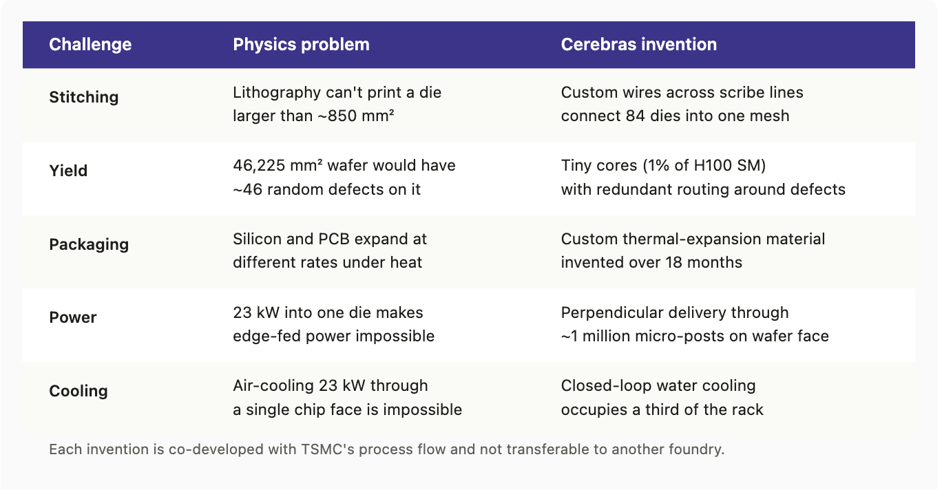
Five engineering inventions: the physics problem and Cerebras’s solution at each layer
What matters isn’t any single one of these. It’s that each was co-developed with TSMC’s specific process flow, defect maps, and packaging capabilities — and none of them transfers to Samsung Foundry, Intel Foundry Services, or any other fab.
Lior Susan at Eclipse — whose $147M total investment in Cerebras returned $2.5 billion at IPO — put the broader version of this argument cleanly on stage this week:
the real moat in software is gone. You can vibe code pretty much whatever you want. What you cannot do with vibe code is manufacture wafers, because you need machines and silicon, and they need clean rooms, and a bunch of other things.
Susan is naming the right level of the argument. The deeper read is one layer below: it's not just that wafer manufacturing is a moat — it's that this specific wafer manufacturing flow exists nowhere except inside Cerebras's ten-year partnership with TSMC.
This is the deepest part of the moat, and it’s what almost no one is naming this week:
Cerebras’s competitive position isn’t wafer-scale as an idea. It’s wafer-scale as a TSMC-co-developed manufacturing flow that compounds in process-years.
A competitor with unlimited capital cannot replicate this by licensing the architecture and going to a different fab. The custom CTE-matched material, the scribe-line lithography accommodation, the perpendicular power delivery integration, and the defect management protocols are TSMC partnership artifacts.
But the more important point is that competitors aren't racing to duplicate wafer-scale. They're pursuing a different physical path to similar system-level performance: high-density SRAM in 3D stacks, glass substrates extending traditional packaging, silicon photonics interconnect, emerging memory architectures. That race is real, and the lead Cerebras has is meaningful but not as long as the wafer itself implies. The deeper truth is that all of these paths require deep foundry co-optimization — what the industry calls DTCO (Design-Technology Co-Optimization), now evolving into STCO (System-Technology Co-Optimization). The moat isn't the wafer. The moat is the depth of the foundry partnership underneath whichever physical path you take.
This is the most important lesson for constraint-layer investing in the next decade:
The deepest moats in deep tech are foundry partnership depths, measured in process-years, not patents.
Why this matters for what we’re building at Good AI
Two weeks ago, I was in Hong Kong with our partners, hosting LP conversations at Sidley Austin’s offices at Two IFC. The thesis we presented over the course of that week was simple:
Good AI invests in the constraint layer of AI — power, capacity, and trust. That’s where the next wave of value will concentrate, and we back the founders solving those bottlenecks.
The framing we used to anchor those conversations was a Public–Private Bridge — the thesis that what LPs already own in their public portfolios maps directly to what we’re underwriting at the seed stage.
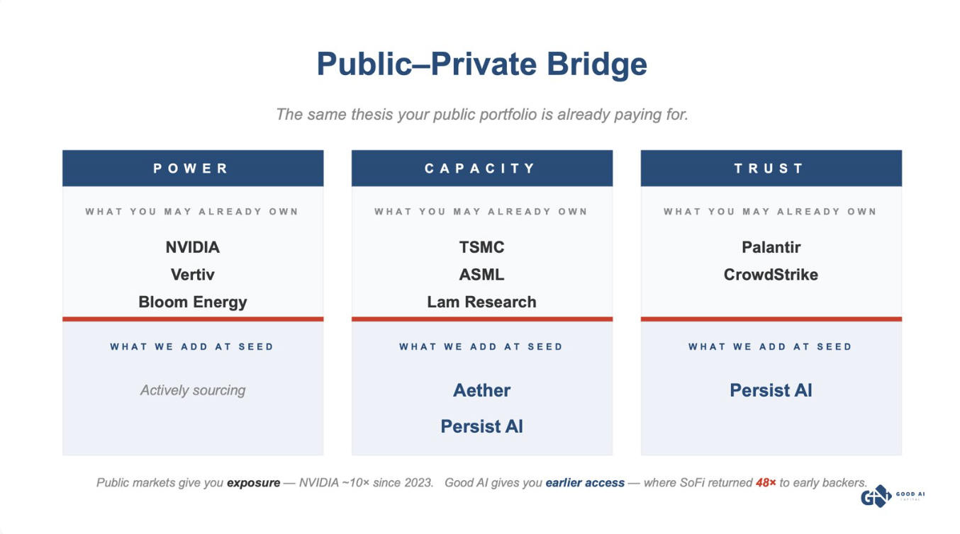
Public-Private Bridge: the framework we presented to LPs in Hong Kong, two weeks before the Cerebras IPO. Image: Good AI Capital
When we wrote that slide, TSMC was the public-market anchor for the Capacity pillar — the company whose foundry partnership and advanced packaging IP makes everything from CoWoS-enabled GPU systems to AMD’s MI series possible. We didn’t anticipate that within two weeks, the most consequential public validation of the entire framing would come from a different angle: a wafer-scale processor whose entire commercial viability depends on the same TSMC partnership we’d already centered in our LP narrative.
That’s the value of having a thesis. Cerebras isn’t one of the constraint-layer companies we’re tracking. It’s the public proof that the framework prices correctly.
The companies we’re backing at the seed stage are the same thesis shape at the earliest stage. Aether Biomachines is using AI to design and manufacture advanced materials for 3D printing — dual-use applications spanning industrial manufacturing and defense. The constraint they’re attacking is the gap between what AI models can predict about materials at the simulation layer and what can actually be manufactured at industrial scale. Their bet is structurally the same as Cerebras’s: build the manufacturing process alongside the AI, not after it. That’s the kind of integrated physical-AI bet that doesn’t compress into a five-year cycle.
Persist AI sits on the Trust pillar — making pharmaceutical formulation auditable and reproducible at AI-scale, the constraint that makes deployed AI in regulated industries actually work.
Cerebras at $95 billion is the public-market verdict on the framework. Aether and Persist are the same thesis at the seed stage, in different domains.
What this means for the next five years
Constraint-layer investing isn’t picking the next NVIDIA-killer. It isn’t betting on a single architecture. It’s a method:
1. Identify the binding bottleneck. Memory bandwidth for inference. Power and cooling for data centers. Manufacturing yield for advanced silicon. Trust and auditability for deployed AI in regulated industries. The bottleneck is rarely the technology everyone is debating; it’s usually one layer beneath that.
2. Underwrite the process-IP moat, not the architectural insight. Wafer-scale was a known idea for forty years. The TSMC partnership was the moat. The same logic applies to advanced packaging, photonic interposers, novel battery chemistries, and most physical-process bets. The semiconductor industry has a name for this: System-Technology Co-Optimization (STCO) — the recognition that design, fab process, and packaging can't be optimized independently anymore. The idea isn't defensible. The decade of co-developed STCO is.
3. Back founders willing to spend a decade. Cerebras took ten years from term sheet to IPO. Aether will take similar. Persist will take similar. These are not five-year flips. They are generational bets, and the funds that win them are the funds that can hold conviction through long uncertainty.
4. Early entry compounds dramatically. Cerebras’s Series A was priced at $0.85 per share in 2016. The IPO priced at $185. That’s a 218x multiple captured by the earliest believers — Foundation, Eclipse, and Benchmark. Growth funds entering at Series H paid roughly $89 per share for the same architectural insight, capturing about 2x. The math of constraint-layer investing is the math of conviction held at maximum uncertainty.
Congratulations to Andrew Feldman and the entire Cerebras team. Congratulations to Steve Vassallo at Foundation, Lior Susan at Eclipse, and every investor whose conviction at the earliest stages made this IPO possible.
The constraint layer is real. The market is large. The framework prices correctly.
We’re just getting started.
Sidebar: How wafer-scale silicon actually gets made
To understand why Cerebras is technically extraordinary, it helps to understand how chips normally get made — and what step Cerebras skips.
From sand to silicon. Pure silicon is melted and grown into a long cylinder using the Czochralski process: a seed crystal is dipped into molten silicon and slowly pulled upward while spinning. The silicon cools and solidifies into a flawless ingot, roughly 12 inches in diameter. Wire saws then slice the ingot into thin, round wafers, like cutting a salami.
Printing the chips. Lithography machines built by ASML use ultraviolet light to print billions of microscopic transistor patterns onto the wafer. Because a single GPU or CPU is much smaller than a 12-inch wafer, the machine prints a grid of identical rectangular chip patterns across the wafer’s surface. Each rectangle is called a die.
The cut. Once the wafer has been fully patterned, a diamond saw or laser slices along the grid lines — a process called dicing. Each individual die is separated from its neighbors, tested, and packaged into the protective housing you’d recognize as an NVIDIA B200 or an Intel CPU.
Why wafers are big. You can't simply grow tiny wafers for tiny chips — silicon must be grown in large, perfectly round ingots, and the physics doesn't allow shortcuts. A leading-edge 2nm or 3nm logic fab costs $25–30 billion to build today. The machinery takes the same time and energy to process a wafer whether it contains one chip or a thousand. Big wafers exist because the fixed costs of manufacturing demand maximum chip density per wafer.
What Cerebras does differently. They don’t dice. The entire 12-inch wafer remains intact as a single processor.
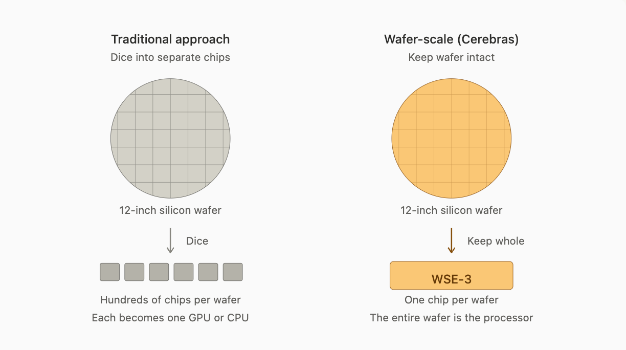
Same wafer, different end product: traditional dicing vs Cerebras wafer-scale
The hard part isn’t deciding to skip the cut. It’s making the resulting “chip” actually work:
Defects. On a normal wafer, scattered defects affect a percentage of individual dies. Modern designs handle this gracefully — an NVIDIA H100 with a localized defect can fuse off the broken core and ship anyway. But a single catastrophic defect zone anywhere on a 12-inch monolithic chip would traditionally scrap the entire wafer. Cerebras solves this by making each AI core extremely small — roughly 1% the size of an H100 core — and building in redundant routing across the whole wafer, so defects get routed around like bad blocks on a hard drive.
Connecting the dies. Lithography limits mean Cerebras still prints 84 separate dies on the wafer. They then add custom lithography steps to pattern over a million wires across the scribe lines, making all 84 dies behave as one seamless mesh. Software sees one chip, not 84.
Packaging. Instead of putting a small silicon square into a plastic cartridge, the entire wafer is sandwiched into a custom-engineered frame that delivers 23 kilowatts of power perpendicularly into the wafer face and circulates water against the back for cooling.
What Cerebras built isn’t a chip. It’s an entire compute system implemented on a single continuous piece of silicon, with the packaging, power delivery, and cooling all custom-engineered around that constraint.
That’s the technical achievement. The commercial moat is that it took ten years and a decade-long TSMC partnership to make it actually work at yield.